
-
Please try to be as accurate as possible with your search.
-
We can quote you on 1000s of specialist parts, even if they are not listed on our website.
-
We can't find any results for “”.
How to Select a Digital Output Module for Load Switching Capacity
Digital output modules look simple on a catalog page. You see voltage, current, and channel count, and it is tempting to pick the cheapest part that meets those numbers. In real plants, that shortcut is how you end up with welded outputs, nuisance trips, or output cards that cook themselves in a hot cabinet after a few months of service.
From a systems integrator’s standpoint, selecting the right digital output module is fundamentally a load‑switching problem. The question is not “Can this module turn on?” but “Can this module switch these specific loads, under these conditions, for years, without degrading the rest of the system?”
In this article I will walk through how I approach digital output selection for load switching capacity, using practical criteria rather than marketing labels, and leaning on guidance from sources such as PLCDesign, NI, RealPars, Cadence, Sealevel, NASA, and Monolithic Power Systems.
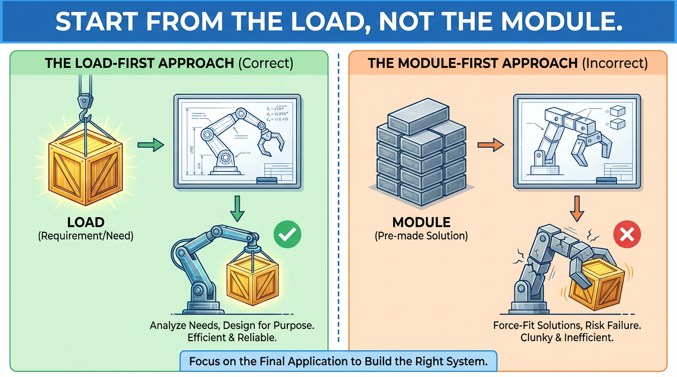
Start from the Load, Not the Module
Every good design starts with the field devices, not with a rack catalog. PLCDesign makes this point clearly: I/O module selection should balance technical requirements, overall solution cost, and any approved‑manufacturer constraints, rather than focusing on module price alone. For digital outputs, that means you first characterize what you are switching.
Begin by listing each load: solenoid valves, contactor coils, beacons, alarms, motor starters, DC motors, and any specialty actuators. For each device, note the rated supply voltage from its datasheet and identify whether it is AC or DC. PLCDesign notes that digital output voltage is most commonly 24 VDC, but that 120 VAC, 240 VAC, or 125 VDC outputs are often required to match field devices such as solenoids, lamps, and motor control centers. Technology‑style guidance on flex modules likewise highlights typical bands like 12–24 VDC and 120–240 VAC, so your load list should reflect those ranges.
Next, identify the steady‑state current of each load. You do not need to guess values; you need the manufacturer’s numbers. PLCDesign emphasizes that the power of the final element, defined by its supply voltage and current, is what drives output module choice and whether interposing relays are needed. If a load requires more current than any available solid‑state output can handle, or if its inrush is unknown, you are already in the domain where you should be thinking about interposing relays or dedicated drivers.
Finally, note how often each load will switch. Many designers forget that switching frequency is part of load switching capacity. PLCDesign explicitly calls out that high switching‑frequency applications require checking the module’s maximum output frequency and managing overvoltage from inductive loads such as contactors and coils. A lamp that turns on twice a day is a different design problem from a small valve that actuates several times per second.
By the time you have voltage type, current, and switching frequency per load, you have enough information to choose output technologies and start considering margins.
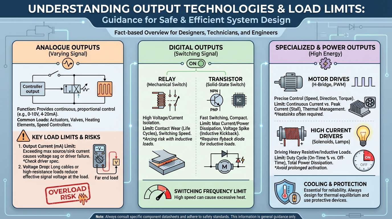
Understand Output Technologies and Their Load Limits
Industrial digital output modules rely on three core switching technologies: mechanical relays, transistors, and triacs. RealPars provides a clear breakdown of how PLC manufacturers use these technologies, and PLCDesign echoes that the internal output component type is critical for module selection.
Relay outputs
Relay output modules use miniature electromechanical relays with coils and contacts. RealPars notes that these relay outputs are effectively voltage‑independent: they can switch AC and DC loads, and even mix them on different channels in the same module. The relay provides galvanic isolation and very low on‑state resistance when closed, so you see minimal voltage drop across the contacts and can often switch comparatively higher currents than with a transistor or triac card.
The tradeoffs show up in speed and lifetime. RealPars points out that relay outputs are slow, with response times on the order of about ten milliseconds or more, and the mechanical contacts are subject to wear. PLCDesign warns that relay outputs in high‑density modules can suffer thermal issues in long‑on‑time applications and have lower mean time between failures, so their use “must be justified.” Contacts that repeatedly interrupt inductive loads experience arcing and erosion, which the Sealevel application note on switching inductive loads illustrates vividly: using a reed relay to interrupt a 24 V DC motor produced voltage spikes up to roughly 200 V at the relay terminals. That stress shortens relay life if you do not add proper suppression.
Relay outputs are therefore best reserved for situations where you must switch mixed AC and DC voltages, where you require true galvanic isolation, or where you have higher‑current loads at modest switching frequencies and you are willing to accept mechanical wear. They are not ideal for high‑speed, high‑cycle‑count control of inductive loads without extra protection.
Transistor outputs
Transistor output modules are solid‑state devices intended for DC loads. RealPars explains that these outputs are voltage‑dependent and require correct polarity. They are built either as sourcing outputs, which provide positive voltage to the load, or as sinking outputs, which provide a path to ground.
RealPars also notes that transistors are not ideal switches: they exhibit a small voltage drop when on and a leakage current when off. That leakage can matter for sensitive loads or devices that interpret very small currents as a valid “on” state. The Sealevel note shows a practical variant of transistor outputs: open‑collector outputs with integrated flyback diodes, designed specifically to drive inductive loads such as DC motors. In the same 24 V DC motor test where reed relay contacts saw about 200 V spikes, the open‑collector output with a flyback diode limited the voltage change at the output terminal to roughly 30 V when turning off. That is a dramatic reduction in stress on both the output device and the motor.
At the device level, Cadence compares Darlington transistor stages and MOSFETs for switching. Darlingtons provide very large current gain from small input currents but suffer from higher saturation voltage and power loss, and they turn off slowly. MOSFETs, by contrast, are gate‑voltage‑controlled devices with essentially no steady‑state input current, and the Cadence guidance notes that MOSFETs are generally far more efficient and have become the default choice in modern digital switching circuits. When you buy a transistor output module from a major vendor, you are typically buying arrays of MOSFETs and associated drivers, not discrete Darlington pairs, precisely for these efficiency and speed reasons.
For load switching capacity, transistor outputs are ideal when you have DC loads that need fast response, where you can accept the on‑state voltage drop and off‑state leakage and where per‑channel current is moderate. They are a natural fit for solenoids, small contactor coils, and moderate DC motors when combined with proper inductive suppression.
Triac outputs
Triac outputs are solid‑state devices dedicated to AC loads. RealPars explains that triac modules switch faster than relays and are typically suited for low‑power AC applications such as lighting circuits, motor starters, and contactors, with typical current ratings around 1 A per channel. Because triacs rely on alternating current zero crossings to turn off, they cannot properly interrupt DC loads, which is why they are reserved for AC.
If your loads are exclusively AC and relatively modest in current, a triac module gives you solid‑state reliability and speed without the mechanical wear of relays. For larger AC motor starters and mixed‑voltage loads, relay modules or separate contactors remain more appropriate.
Comparing the technologies
The decision between relay, transistor, and triac is not abstract; it is about what you can reliably switch for the long term. The following table summarizes the practical differences, based on the RealPars and PLCDesign guidance and the Sealevel inductive load data.
| Output technology | Load voltage type | Strengths for load switching | Main limits and risks |
|---|---|---|---|
| Relay | AC and DC, mixed across module | Voltage‑independent contacts, galvanic isolation, comparatively high current capability | Slow response, mechanical wear, thermal concerns in dense cards, severe stress without inductive suppression |
| Transistor | DC only | Fast switching, long lifetime, easy interfacing to digital logic, excellent with flyback diodes | Limited current per channel, on‑state voltage drop, off‑state leakage current that can upset very sensitive loads |
| Triac | AC only | Fast switching for AC loads, solid‑state reliability for low‑power lighting and coil circuits | AC‑only operation, typical per‑channel current around 1 A, requires proper AC load characteristics for safe turn‑off |
Once you know what class of output technology fits each group of loads, you can focus on the real heart of the question: how much capacity you actually have and what margin you need.
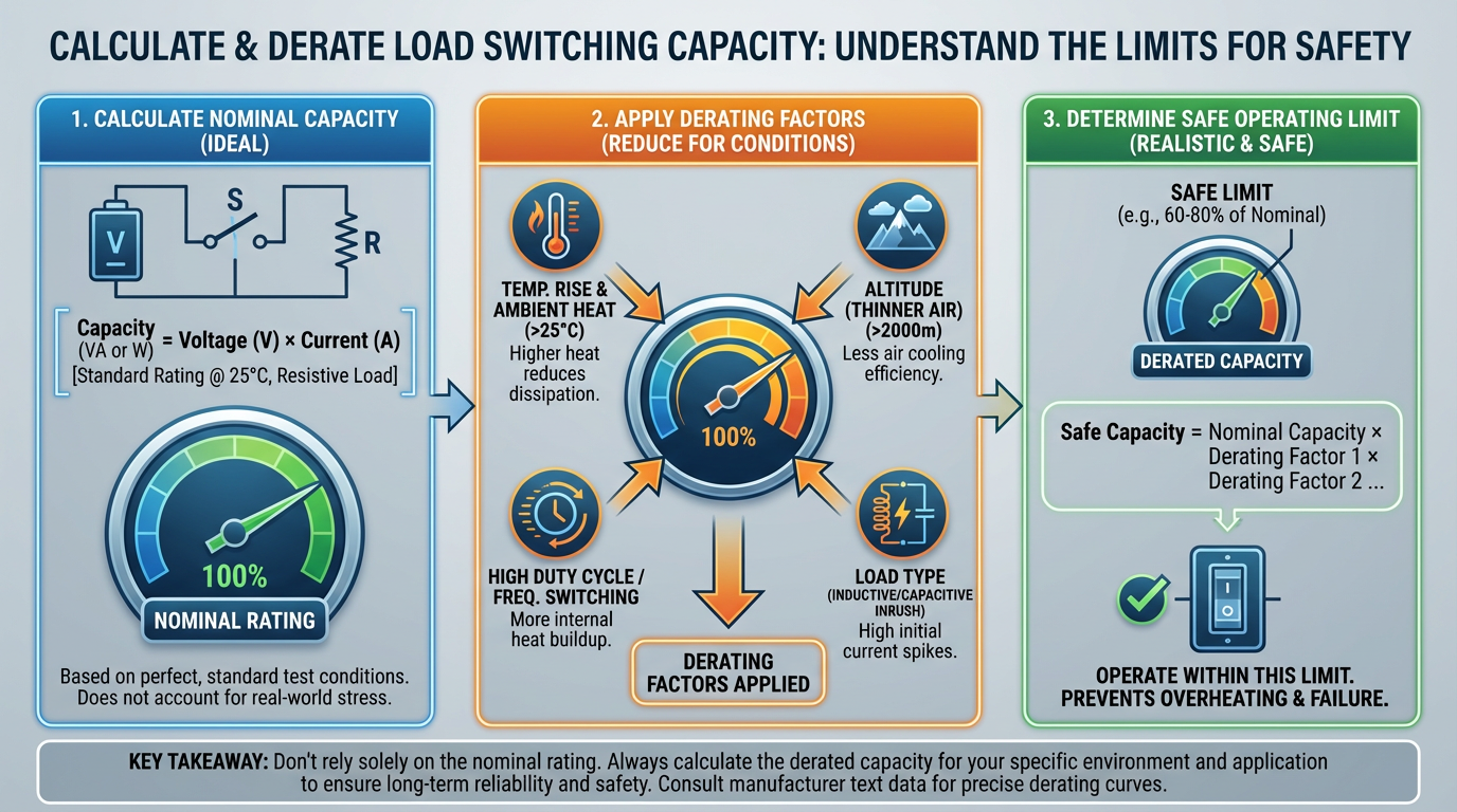
Calculate and Derate Load Switching Capacity
A digital output’s nameplate ratings tell only part of the story. Monolithic Power Systems emphasizes in its power electronics design guidance that efficiency and reliability depend on minimizing conduction and switching losses and on proper thermal management and derating. They give a concrete example: running a MOSFET at about seventy percent of its maximum current rating significantly reduces junction temperature and failure risk from overcurrent or thermal stress.
Digital output modules that rely on MOSFETs or other solid‑state devices follow the same physics. If a card is rated for a certain current per channel, consider how that rating was defined. Was it at a specific ambient temperature? Was it with only one channel energized, or all channels loaded? Many vendors specify both per‑channel and per‑module limits. Operating every channel continuously at the absolute maximum current, in a warm cabinet, is how you turn a perfectly good specification into a derating failure.
A pragmatic way to treat load switching capacity is to use the vendor’s continuous ratings as hard ceilings but design your load assignments so that typical steady‑state currents are closer to the comfortable margin Monolithic Power discusses. If a module channel is rated for a certain current and your load pushes right to that number in steady operation, consider either moving that load to a higher‑capacity module, spreading loads across multiple cards, or using an interposing relay or driver that moves the heavy lifting off the PLC backplane.
Switching frequency matters as well. Every transition dissipates switching energy in the transistor or relay. PLCDesign explicitly recommends checking a module’s maximum output frequency for high‑frequency applications. A fast‑cycling valve bank, a pulsed test system, or a drive that uses PLC outputs for chopper‑like signals will stress outputs differently from a slow‑cycling interlock. For high‑speed use, you should confirm that the module’s specified switching frequency and thermal behavior match your application.
There is also the question of simultaneous load. The Technology.org discussion of flex digital output modules notes that designers should consider channel density and power consumption, because the total power drawn by the module can impact the backplane or network power. If you place every high‑current load on the same card and drive them simultaneously, you may hit the module’s total current limit, even if each individual channel is within spec. A conservative design distributes high‑power loads across cards and leaves headroom on both per‑channel and aggregate ratings.
Manage Inductive Loads and Transients
Load switching capacity is not only about steady current; it is about what happens when you turn a load off. Inductive loads store energy in their magnetic fields. When you interrupt that current, the energy has to go somewhere, and it appears as voltage.
Sealevel’s test on switching highly inductive loads with digital I/O demonstrates this clearly. In a setup where a SeaI/O relay module switched a 24 V DC motor, oscilloscope measurements at the relay terminals showed voltage spikes routinely around 200 V when the relay opened, with a typical change of about 127 V. That is an order of magnitude above the supply voltage, and exactly the kind of stress that causes relay contact arcing, possible contact fusing, and damage to surrounding circuitry.
The same motor, when switched using an open‑collector transistor output module with an integrated flyback diode on each channel, produced a maximum observed voltage change of only about 30 V at the output terminal when power was removed. The difference is that the flyback diode provided a safe path for the inductive current to continue flowing and dissipating energy instead of forcing the relay or transistor to absorb the entire voltage spike.
Basic switching circuit theory, as discussed in the relay‑switch tutorial from Basic Electronics Tutorials, reinforces this picture. A relay coil is an inductor; when a bipolar transistor or MOSFET turns off, the collapsing magnetic field drives the current into a high reverse voltage across the coil. A flywheel, or flyback, diode across the coil clamps this reverse voltage to about a diode drop, around 0.7 V, protecting the switching device. For AC coils the same tutorial points to RC snubber networks because diodes only apply cleanly in DC circuits.
From a module selection standpoint, this means that load switching capacity must be considered together with inductive energy handling. Modules designed for inductive loads often advertise integrated flyback protection or snubbers. Sealevel’s open‑collector modules with onboard flyback diodes are one explicit example. ProtoExpress’s design best practices emphasize adding flyback diodes across relay coils and appropriate surge and over‑voltage protection as part of robust circuit design. If your loads are motors, large solenoids, or big contactor coils, a “bare” relay output without suppression is a risk. Either choose digital output modules that integrate appropriate inductive protection or plan to add external diodes or snubbers at the field terminals.
The bottom line is that switching capacity is not just continuous current and voltage; it is the ability of the output and its protection network to survive repeated energy dumps from inductive loads without failing or generating electromagnetic interference that upsets nearby circuits.
Sinking vs Sourcing and 2‑Wire vs 3‑Wire Constraints
The way current flows through a digital output channel and its load has a direct impact on what that channel can safely switch. The SMDSensors guidance on sinking versus sourcing digital outputs explains that a sourcing output provides positive voltage to the load, while a sinking output provides a path to ground but does not supply power itself. Matching these correctly to the inputs or loads they drive is essential: a sourcing output must feed a sinking input or load, and a sinking output must be paired with a sourcing input that provides the voltage.
This pairing affects load switching capacity in subtle ways. In a sourcing output configuration, the module is responsible for supplying the full load current at the supply voltage. In a sinking configuration, the module must be able to sink the full load current to ground. From the perspective of the semiconductor devices inside the module, the stress is similar, but the wiring determines whether the output must tolerate additional ground noise or shared return paths.
NI’s application note on choosing the right industrial digital I/O module for digital output sensors highlights another dimension: the behavior of 2‑wire and 3‑wire devices in their off and on states. For 2‑wire devices, NI points out that even when the sensor is “off,” it draws a small residual current, often called off‑state leakage or residual current, to keep its electronics powered. They note that most industrial 2‑wire sensors have off‑state leakage no higher than about 1.7 mA. In the on state, a 2‑wire sensor requires a minimum holding current, typically in the range of 3 to 20 mA, to remain activated. If the digital I/O module cannot sink or source at least that current, the sensor will not operate reliably.
For 3‑wire, line‑powered sensors, NI explains that the device takes its power from a dedicated excitation terminal, and the current drawn from the I/O line is mainly a burden current, typically around 20 mA. The key recommendations are that the module’s leakage current tolerance must exceed the sensor’s residual current to avoid false on states, and its current capability must meet or exceed the sensor’s minimum holding or burden current.
Although NI discusses sensors driving digital inputs, the same currents and leakages apply when digital outputs are used as supply or load paths. When you select a digital output module to switch power to small 2‑wire devices, you should verify that any off‑state leakage from a transistor output will not inadvertently power the device, and that the channel can supply the minimum holding or burden current in the on state. RealPars’ observation that transistor outputs themselves have leakage in the off state reinforces the need to consider both sides of the loop.
In practice, this means reading both the load’s datasheet and the output module’s specifications for off‑state leakage, minimum load, and maximum sink or source current. A mismatch can leave you with loads that never quite turn off, or sensors that never quite turn on.
Distance, Noise, and Environment
Electrical ratings on paper assume ideal conditions. In industrial plants, conditions are rarely ideal. PLCDesign notes that higher‑voltage digital outputs without interposing relays are mainly justified when field devices are far from the cabinet, electromagnetic noise is high, loads are high power, or environments are dirty or dusty and stress electrical contacts. That is a concise description of many process plants.
Higher voltages are attractive over long cable runs because they reduce relative voltage drop and improve noise immunity. PLCDesign points out that current‑loop standards like 4–20 mA can reach long distances on the order of more than half a mile at 24 VDC while maintaining signal integrity, whereas voltage‑based analog ranges suffer from cumulative drops over junction boxes. Although digital outputs are not analog loops, the same wiring realities apply. A 24 VDC output switching a distant device over a long cable has to contend with resistive voltage drop, capacitive and inductive coupling, and transients induced by nearby equipment.
NASA’s high‑speed PCB design guidance adds another dimension: edge rates, not nominal frequency, define when interconnects behave like transmission lines. While most digital outputs in industrial control are relatively slow compared to gigahertz RF, modern solid‑state outputs can have sharp edges that generate significant high‑frequency content. NASA’s recommendations about controlled impedance, short and direct routing, and continuous reference planes are aimed at high‑speed boards, but the underlying principle is the same in I/O modules and their backplanes: fast switching into long, poorly terminated cables is a recipe for reflections and electromagnetic interference.
Monolithic Power Systems and ProtoExpress both emphasize electromagnetic compatibility and grounding. They recommend minimizing high‑current loop area, providing robust decoupling near power pins, and using appropriate filters and surge suppression to control conducted and radiated noise. From a selector’s perspective, this translates into favoring digital output modules that are explicitly designed and certified for noisy industrial environments and that include appropriate EMC and surge protections rather than bare‑bones cards meant only for benign lab conditions.
Finally, environmental factors like temperature and contamination come back to thermal and mechanical stress. PLCDesign warns about thermal issues in high‑density relay modules, and Monolithic Power’s derating advice shows how temperature and current interact. In dusty, dirty, or corrosive atmospheres, relay contacts and exposed connectors deteriorate faster. In such environments, a solid‑state output module or an isolated module located in a cleaner intermediate cabinet can pay for itself in reduced maintenance.

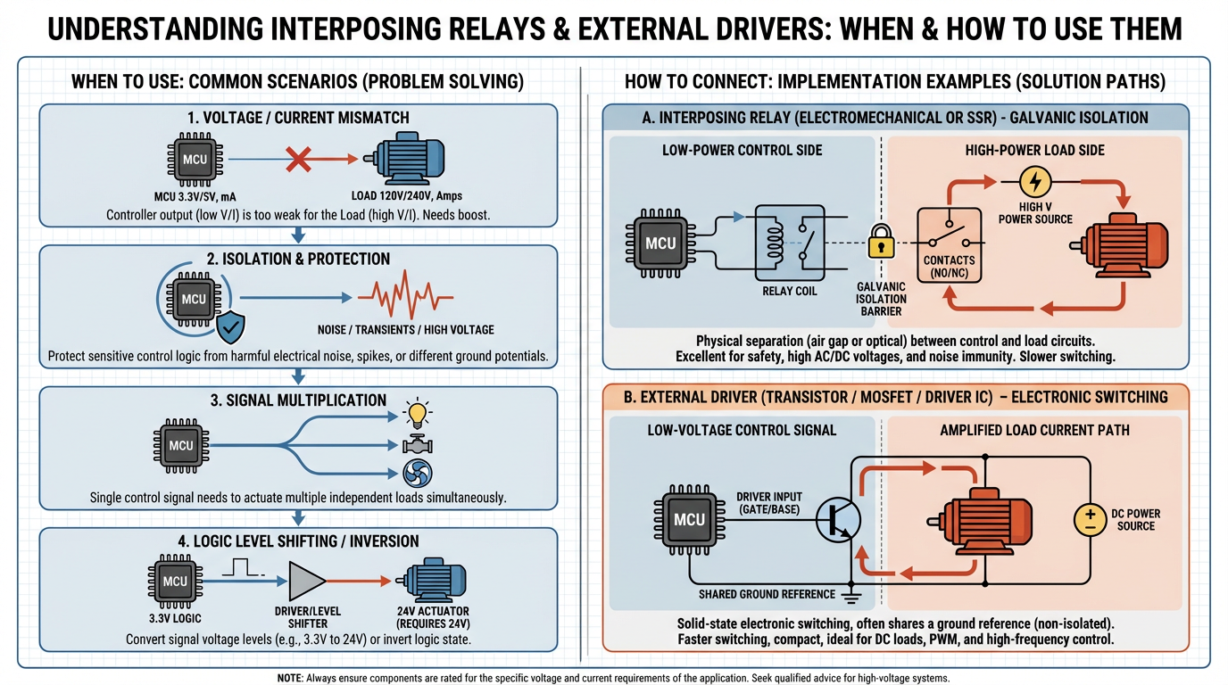
When and How to Use Interposing Relays or External Drivers
Interposing relays remain a core tool in the integrator’s kit, despite the availability of high‑current solid‑state modules. PLCDesign describes interposing relays as a way to electrically isolate cabinets from field devices, adapt to different field voltages, handle high‑current loads, fan out one PLC output to several field elements, or provide voltage‑free contacts. The cost of each extra relay is more than just hardware; each relay is another failure point that must be considered in availability calculations, especially in redundant systems.
The relay‑switch tutorial from Basic Electronics Tutorials shows the typical transistor or MOSFET driver circuits used to energize relay coils, with flyback diodes or snubbers to handle inductive energy. In many OEM digital output modules that integrate relays, these driver circuits are already on the card. When you add interposing relays in the field marshalling, you are essentially duplicating those stages externally. There is nothing inherently wrong with that, provided you account for space, power, and reliability.
Use interposing relays when your loads require voltages or currents beyond the safe switching capacity of any available digital output module, when you must interface to field wiring standards that differ from the PLC’s rated voltage, or when you need special contact forms such as changeover contacts that the module does not provide. In those cases, treat the digital output as a logic‑level control signal and keep its load limited to the coil current of the interposing relay, which is usually modest compared with the final field device.
Conversely, avoid reflexively adding relays in environments where solid‑state outputs already provide adequate isolation, current capacity, and inductive suppression, particularly for DC loads. Sealevel’s tests and the general power‑electronics guidance from Monolithic Power and ProtoExpress make clear that properly designed transistor outputs with correct protection can switch inductive loads repeatedly with less wear and less electromagnetic noise than mechanical contacts.
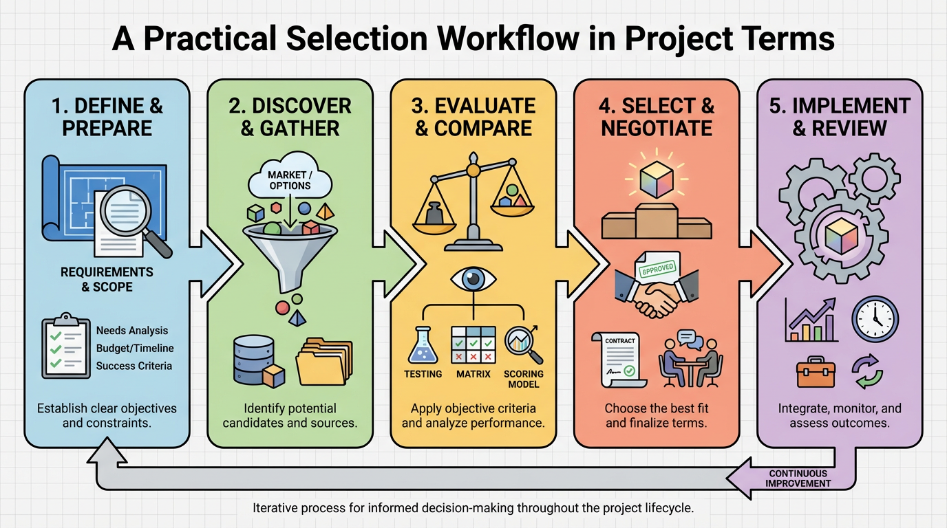
A Practical Selection Workflow in Project Terms
In real projects, I do not start with “Which card is cheapest?” I start with a load list and then work backward to the appropriate outputs.
The first pass is about grouping. Once the load list is built, I group loads by voltage and by AC or DC. That very quickly suggests which racks or remote I/O stations need 24 VDC transistor outputs, which need 120 or 240 VAC triac or relay outputs, and which places truly require mixed voltages and therefore relays.
The second pass focuses on current and duty cycle. For each group, I sum the worst‑case currents and compare them to available modules’ per‑channel and per‑module ratings, remembering the derating guidance from Monolithic Power. If I see any loads that drive a channel close to its maximum continuous rating, particularly at high duty cycle, I consider moving them to a higher‑capacity module or putting an interposing relay in front of them. If several high‑current loads would land on the same card, I redistribute them so the cards are not thermally or electrically overloaded.
The third pass is about load type and protection. I tag inductive loads and cross‑check whether the selected modules provide appropriate protection. The Sealevel results are a reminder that a motor or large inductive load will happily generate several times the supply voltage as a spike when you turn it off. If the card is not explicitly designed for inductive loads, I plan for external flyback diodes on DC coils or RC snubbers on AC coils and ensure there is space in the marshalling to mount them.
The fourth pass looks at wiring topology. Using the SMDSensors guidance, I verify whether each device is sinking or sourcing and ensure the I/O module type matches, so I do not inadvertently pair a sinking output with another sinking device. For any 2‑wire or 3‑wire devices, I refer back to NI’s current and leakage recommendations to make sure the chosen module will not misinterpret residual currents or fail to provide the holding current the device expects.
The final pass considers environment and life‑cycle. Here I weigh whether relay modules will see so many operations or such severe conditions that their mechanical wear becomes a concern, in which case solid‑state alternatives or interposing solutions may make more sense. I also consider future expansion and spares strategies, following the approach described in flex module selection guidance, where you balance technical specs with vendor support, lead times, and total cost of ownership.
By the end of this workflow, the choice of digital output modules is no longer a guessing game; it is a set of justified decisions tied back to specific loads, environments, and reliability goals.
Brief FAQ
How much margin should I leave on digital output current ratings?
Monolithic Power’s power‑electronics guidance suggests running MOSFETs at roughly seventy percent of their maximum current rating to reduce junction temperature and extend life. For digital output modules that rely on similar devices, I treat that as a good engineering target rather than driving channels at their absolute maximum. If a channel will spend long periods near its rated limit, especially in a warm cabinet, I either move that load or add an interposing driver.
Can I avoid interposing relays by just buying higher‑current digital output modules?
Sometimes you can, but not always. PLCDesign notes that higher‑voltage or higher‑power outputs without interposing relays are justified when field devices are far from the cabinet, the environment is noisy, or loads are high power. However, each output technology has limits: triac modules are usually around 1 A per channel, transistor modules have per‑channel and total limits, and relay contacts will still wear when switching inductive loads. Even a high‑current output card benefits from sharing duty with interposing relays when switching large motors, heavy contactors, or when you need special contact forms or isolation schemes.
What is the biggest pitfall in load switching capacity you see on projects?
The most common pitfall is ignoring transient and lifetime behavior. Designers often size outputs for steady‑state current at room temperature and forget about inductive kick, duty cycle, ambient temperature, and simultaneous loading. That is how you end up with outputs that pass factory tests but fail after a year in a real plant. Treating load switching capacity as a long‑term thermal and transient problem, not just a static current rating, avoids most of those surprises.
In the end, the digital output module is your system’s handshake with the physical world. If you respect the loads, the physics, and the guidance from sources such as PLCDesign, NI, RealPars, Cadence, Sealevel, NASA, and Monolithic Power Systems, your outputs will quietly do their job for years. That is what a reliable project partner is supposed to deliver.
References
- https://s3vi.ndc.nasa.gov/ssri-kb/static/resources/High-Speed%20PCB%20Design%20Guide.pdf
- https://vtechworks.lib.vt.edu/bitstream/handle/10919/31205/thesis.pdf
- https://www.technology.org/2025/10/07/how-to-choose-flex-digital-output-modules-efficiently/
- https://www.researchgate.net/publication/279166628_Modelling_and_Performance_Analysis_of_a_Digital_Switching_System-Case_Study_of_the_C-DoT_DSS
- https://www.sealevel.com/how-to-switch-highly-inductive-loads-using-digital-io?srsltid=AfmBOoq3ZP3IzmBe14BKf-jVfZx9_H_YnR9kzCmrni8Cz2Ub1TfyR3TV
- https://resources.pcb.cadence.com/blog/2023-pdarlington-transistor-vs-mosfet-selection-guidelines
- https://www.electronics-tutorials.ws/blog/relay-switch-circuit.html
- https://www.realpars.com/blog/plc-output
- https://www.otomasyonline.com/download/Keba/DM%20276A%20%20Digital%20Input-Output%20Module.pdf
- https://plcdesign.xyz/en/selection-io-modules-design-phases/
Keep your system in play!
Top Media Coverage
Categories


Related Products
-
 PROXPAC XL Proximity TransducerAssemblyManufacturer: Bently Nevada
 -
CPU Processor ModuleManufacturer: General Electric
-
 Compact universal controllerManufacturer: Siemens
 -
 Compact current relayManufacturer: ABB
 -
CONTROL MODULEManufacturer: Siemens
-
CPU MODULEManufacturer: Siemens
-
 MODULE CARRIERManufacturer: Emerson
 -
 RESOLVER / DRIVE MODULEManufacturer: Reliance Electric
 -
CLOSED LOOP CONTROL MODULEManufacturer: Siemens
-
 CPU MODULEManufacturer: Siemens

Related articles Browse All
-
 amikong NewsSchneider Electric HMIGTO5310: A Powerful Touchscreen Panel for Industrial Automation2025-08-11 16:24:25Overview of the Schneider Electric HMIGTO5310 The Schneider Electric HMIGTO5310 is a high-performance Magelis GTO touchscreen panel designed for industrial automation and infrastructure applications. With a 10.4" TFT LCD display and 640 x 480 VGA resolution, this HMI delivers crisp, clear visu...
 -
 BlogImplementing Vision Systems for Industrial Robots: Enhancing Precision and Automation2025-08-12 11:26:54Industrial robots gain powerful new abilities through vision systems. These systems give robots the sense of sight, so they can understand and react to what is around them. So, robots can perform complex tasks with greater accuracy and flexibility. Automation in manufacturing reaches a new level of ...
 -
 BlogOptimizing PM Schedules Data-Driven Approaches to Preventative Maintenance2025-08-21 18:08:33Moving away from fixed maintenance schedules is a significant operational shift. Companies now use data to guide their maintenance efforts. This change leads to greater efficiency and equipment reliability. The goal is to perform the right task at the right time, based on real information, not just ...


- Q&A
- Policies How to order Part status information Shipping Method Return Policy Warranty Policy Payment Terms
- Asset Recovery
- We Buy Your Equipment. Industry Cases Amikong News Technical Resources Why choose us
- ADDRESS
-
 32D UNITS,GUOMAO BUILDING,NO 388 HUBIN SOUTH ROAD,SIMING DISTRICT,XIAMEN
Leave Your Comment