
-
Please try to be as accurate as possible with your search.
-
We can quote you on 1000s of specialist parts, even if they are not listed on our website.
-
We can't find any results for “”.
High Resolution Analog Input Module 16‑Bit Accuracy Specification
High‑resolution analog input modules are where a control system either earns its keep or quietly bleeds performance. On paper, “16‑bit accuracy” looks clean and comforting. On the plant floor, where long cable runs, noisy switch‑mode supplies, and crowded cabinets are the norm, that label rarely tells the whole story.
Over the years integrating PLC and DCS systems, I have learned to treat a “16‑bit” spec as the start of a conversation, not the end. Vendors from Apex Embedded Systems to Analog Devices, Contec, and others provide solid building blocks and documentation, but it still takes disciplined engineering to translate their silicon‑level capability into reliable, field‑proven performance.
This article unpacks what “16‑bit accuracy” really means for a high‑resolution analog input module, how to interpret the underlying specifications, and what design and integration practices actually preserve those bits in a real industrial environment.
What A High‑Resolution Analog Input Module Really Is
An analog input module bridges the continuous analog world of sensors with the discrete world of your controller. Contec describes analog I/O as the interface that converts analog sensor signals into digital values a computer can process, and vice versa. In PLCs and DCSs, those signals are typically plant standards such as 4–20 mA current loops, 0–10 V and ±10 V voltage ranges, and in some systems thermocouples and RTDs.
Modern high‑resolution modules build on precision ADCs and carefully designed front ends. Several patterns show up repeatedly in vendor designs.
Apex Embedded Systems, for example, has built custom boards around 24‑bit ADCs for roughly two decades, often engineering them to deliver about 16 bits of noise‑free resolution for demanding measurements. Their examples include isolated STD‑bus and PC/104 cards with sixteen isolated ±10 V or ±50 V inputs, water‑quality boards with 24‑bit converters achieving about ten parts per million precision on ±10 V inputs, and load‑cell cards where the analog section is buried inside a metal can to shield it from noise.
Analog Devices takes a highly integrated approach with devices like the AD4111, a 24‑bit sigma‑delta converter that directly accepts ±10 V voltage inputs and 0–20 mA current inputs from a single 5 V or 3.3 V rail. It embeds high‑impedance dividers, current measurement front ends, open‑wire detection, voltage reference, and clock in one package, and is intended specifically for PLC and DCS input modules.
Speedgoat’s IO109 module shows another end of the spectrum: a 24‑bit sigma‑delta module with twelve differential channels, each with its own converter and two‑pole low‑pass filter, capable of up to 200,000 samples per second and about 93 dB signal‑to‑noise ratio. This type of card is used when you need both high resolution and high sampling rates, such as audio and dynamic structural measurements.
Across these examples, the common thread is that a “high‑resolution analog input module” is not just an ADC. It is a complete signal chain: protection, filtering, isolation, reference and clock circuitry, ADC, calibration logic, and digital interface, all shaped to cope with industrial wiring and noise.
Resolution, Accuracy, ENOB, And Noise‑Free Bits
The first trap with a “16‑bit accuracy” claim is mixing up different concepts. Multiple sources, including Contec and Monolithic Power Systems, emphasize that resolution and accuracy are not the same thing.
Resolution is about how finely you can slice the input range into discrete digital codes. Contec illustrates it with temperature measurement: a 0–100° range measured in 1° steps only needs about eight bits, because that gives 256 codes. Measuring the same range in 0.1° steps needs twelve bits and roughly 4,096 codes. Pushing to 0.01° steps requires sixteen bits and about 65,536 codes.
In other words, a 16‑bit converter can represent roughly sixty‑five thousand discrete steps across its input span. That tells you how small a change in input can, in principle, result in a different digital code, but it does not guarantee that the converter will actually distinguish those steps cleanly in the presence of noise, non‑linearity, and reference drift.
Accuracy is how close the digital output is to the true analog input. Monolithic Power Systems notes that accuracy is usually expressed in least significant bits, percent of full scale, or volts, and it combines several contributors: offset error, gain error, linearity errors such as differential and integral non‑linearity, and noise.
Effective number of bits (ENOB) and noise‑free resolution bridge these two ideas. Practical data‑acquisition articles, including work from NXP and EDN, show that even when you start from an 18‑ or 24‑bit converter, the combination of front‑end noise and converter noise means you only get fewer “usable” bits. Apex calls this out directly: their 24‑bit boards are engineered to yield around 16 bits of noise‑free resolution for industrial measurements.
Noise‑free resolution is the number of upper bits that do not dither as you sit on a constant input. ENOB is a closely related metric derived from signal‑to‑noise ratio measurements. Speedgoat’s IO109, for example, achieves about 93 dB of SNR; that figure, together with the full‑scale range, determines how many bits are truly clean.
A module advertised as “16‑bit accuracy” is therefore making a strong claim. It implies that after you account for offset, gain, linearity, and noise, you can rely on roughly sixteen bits of equivalent resolution over the specified conditions. That usually requires starting from a higher nominal resolution ADC, tight analog design, and careful layout and isolation.
How Real Modules Achieve 16‑Bit Level Performance
When you look at successful high‑resolution modules from vendors and application notes, certain architectural choices repeat. Understanding these helps you judge whether a “16‑bit accuracy” label is credible for your application.
Input Front End And Ranges
Industrial modules must handle standard field ranges. AllAboutCircuits notes that PLC and DCS analog modules typically accept 4–20 mA current loops, 0–10 V or ±10 V voltage ranges, and sometimes wider over‑range to tolerate mis‑wiring.
The AD4111 is a good example of how modern devices simplify this. It accepts ±10 V voltage inputs and current inputs from roughly zero to 20 mA directly, while tolerating a specified over‑range up to about ±20 V and an absolute maximum rating of about ±50 V on the pins. To do this from just a 5 V or 3.3 V rail, it integrates precision resistor networks and current shunts, eliminating the older pattern of external ±15 V buffer amplifiers and discrete dividers.
Contec emphasizes the importance of matching the module input range to the sensor span. If your converter has a 0–10 V range but your sensor only uses 0–5 V, you effectively waste half the codes. They illustrate, for a 12‑bit converter, how halving the range doubles the voltage resolution per step. At sixteen bits, that effect is even more pronounced. A credible 16‑bit module will either offer ranges aligned to common sensor outputs or configurable gain to squeeze more resolution out of smaller signals.
Isolation And Channel Architecture
Isolation strategy is another big factor in whether you can hold 16‑bit‑class performance once the system is wired in a cabinet.
Contec distinguishes non‑isolated, bus‑isolated, and channel‑to‑channel isolated architectures. Non‑isolated modules share ground between field and controller. Bus‑isolated modules isolate the entire bank of analog channels from the backplane, typically using photocouplers to protect the PC or controller from field faults. Channel‑to‑channel isolated modules go further and isolate each input individually with isolation amplifiers so that different channels can float at different ground potentials without interfering.
AllAboutCircuits explains that high‑density PLC and DCS analog cards with eight, sixteen, or thirty‑two channels frequently need channel‑to‑channel isolation in plants with long cable runs, multiple power domains, or hazardous‑area barriers. They highlight that such modules usually target resolutions between sixteen and twenty‑four bits and must meet isolation ratings on the order of kilovolts to satisfy safety standards such as IEC 61131‑2 and IEC 61010.
Apex designs reflect the same trend. They show sixteen isolated ±10 V or ±50 V inputs, isolated 24‑bit channels with configurable sensor bias currents, and load‑cell boards where the entire analog path is inside a shielding can. The pattern is clear: if your application depends on the last few bits of a 16‑bit spec, you want isolation that prevents cross‑talk and ground loops from collapsing those bits under real field conditions.

Integrated Versus Discrete Architectures
Vendors choose between more integrated parts and fully discrete signal chains.
The AD4111 and its pin‑compatible relative AD4112 represent the integrated approach: twenty‑four‑bit ADC, analog front end for voltage and current, reference, clock, and, in the case of AD4111, open‑wire detection, all in one package. Analog Devices reports that the device provides at least about one megaohm of input impedance for voltage channels and publishes total unadjusted error specifications chosen so that many system‑level designs can meet their accuracy requirements without heavy per‑channel calibration. They also built and EMC‑tested a reference board, and documented radiated and conducted immunity and emission results along with layout guidance.
The more discrete approach, as seen in Apex designs or in EDN’s discussion of PLC input chains, builds the front end from dedicated instrumentation amplifiers, filters, and separate ADCs. EDN focuses on selecting low‑noise, low‑drift op amps, especially “multiplexer‑friendly” amplifiers that avoid internal clamp diodes which can otherwise inject charge and slow settling when channels switch between large positive and negative voltages. They also emphasize choosing ADC processes, such as SAR converters in bipolar processes, that offer strong speed‑to‑power performance for multiplexed modules.
Either way can deliver 16‑bit‑class accuracy.
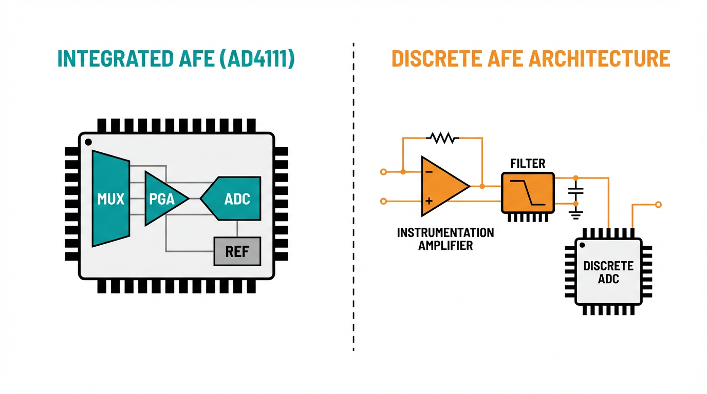
Integrated devices collapse board area and design risk but tie you to a specific architecture. Discrete chains demand more analog expertise but give you flexibility on isolation structure, channel density, and custom ranges.
Layout, Grounding, And Power: Protecting Your Bits
Even the best converter cannot salvage a noisy layout. Both NXP’s ADC design notes and broader PCB guidance from Cadence, Renesas, and ByteSnap converge on several practices that are non‑negotiable when you are chasing 16‑bit‑level performance.
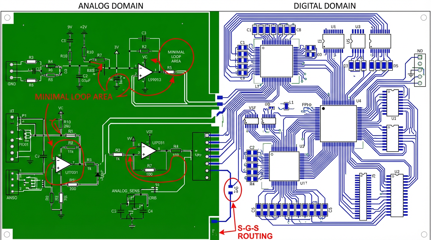
Separating Analog And Digital Domains
Cadence points out that analog circuits have much tighter error margins than digital logic. Digital signals only care about thresholds; analog signals treat every voltage level as meaningful. When you place analog components next to high‑speed digital circuits or let fast digital traces run under analog areas, you invite electromagnetic interference into your measurement path.
The recommended pattern is to group components by function. Power‑conversion components form one cluster. Digital logic such as microcontrollers and communication interfaces form another. Sensitive analog front ends occupy their own region on the board, with physical clearance from both power and digital clusters.
Renesas gives more specific guidance for mixed‑signal MCUs such as the S1JA. They advise using a mostly solid ground plane with a clearly defined analog region, placing the microcontroller, ADC passives, and sensor front ends over a quiet ground area. Analog and digital grounds should be tied together at a single low‑impedance point close to the MCU so that noisy digital return currents do not flow through analog reference nodes.
Grounding, Return Paths, And Loop Areas
NXP’s mixed‑signal article dives deeper into return paths and inductive coupling. High‑speed CMOS logic generates rich high‑frequency harmonics and large transient currents. If analog and digital returns share the same trace or plane segment, those digital currents induce voltage drops that effectively inject noise into analog circuitry.
To reduce this, they recommend not using a single shared return trace for many signals. Instead, route signal‑and‑return pairs tightly coupled to each other, which shrinks the loop area and reduces magnetic coupling. They present an “S–G–S” triplet routing pattern: signal, ground, signal, where the ground trace between analog signals is tied into the ground system at both source and destination.
Renesas and Cadence both stress keeping high‑speed digital traces off analog ground polygons. Even if analog and digital grounds are connected at a single point, running a digital trace over analog ground couples switching currents into that region. Keeping loop areas small and return paths short and direct under the signals helps keep analog measurements stable.
Power Decoupling And Rail Filtering
NXP and ByteSnap both highlight power integrity as a major source of accuracy loss if neglected. Because the supply pin is effectively in series with the analog output, high‑frequency noise on supply rails can couple directly into the converter.
NXP recommends a multi‑stage decoupling strategy around ADCs and mixed‑signal devices. Place a relatively large electrolytic capacitor in the range of about ten to one hundred microfarads within roughly two inches of the chip to handle low‑frequency current swings. Add a small ceramic capacitor between about ten and one hundred nanofarads as close as physically possible to each power pin to shunt high‑frequency noise to ground. Where needed, insert a ferrite bead in series with the supply pin to form an effective high‑frequency choke.
ByteSnap extends this to entire analog rails. For low‑current analog loads, they recommend simple resistor‑capacitor low‑pass filters to clean the rails. For higher current rails, they favor inductors or ferrites with capacitors. They also advocate using parallel capacitors of different values, such as a hundred nanofarads, ten nanofarads, and one nanofarad, in order to create low impedance over a broad frequency range.
On the signal side, ByteSnap suggests filtering sensitive analog lines with ferrite–capacitor networks, choosing cutoff frequencies carefully so that desired signals pass while high‑frequency digital noise is attenuated. They remind designers that sampling frequency should exceed at least twice the filter cutoff to avoid aliasing, echoing the sampling theorem examples that Contec and Monolithic Power Systems explain.
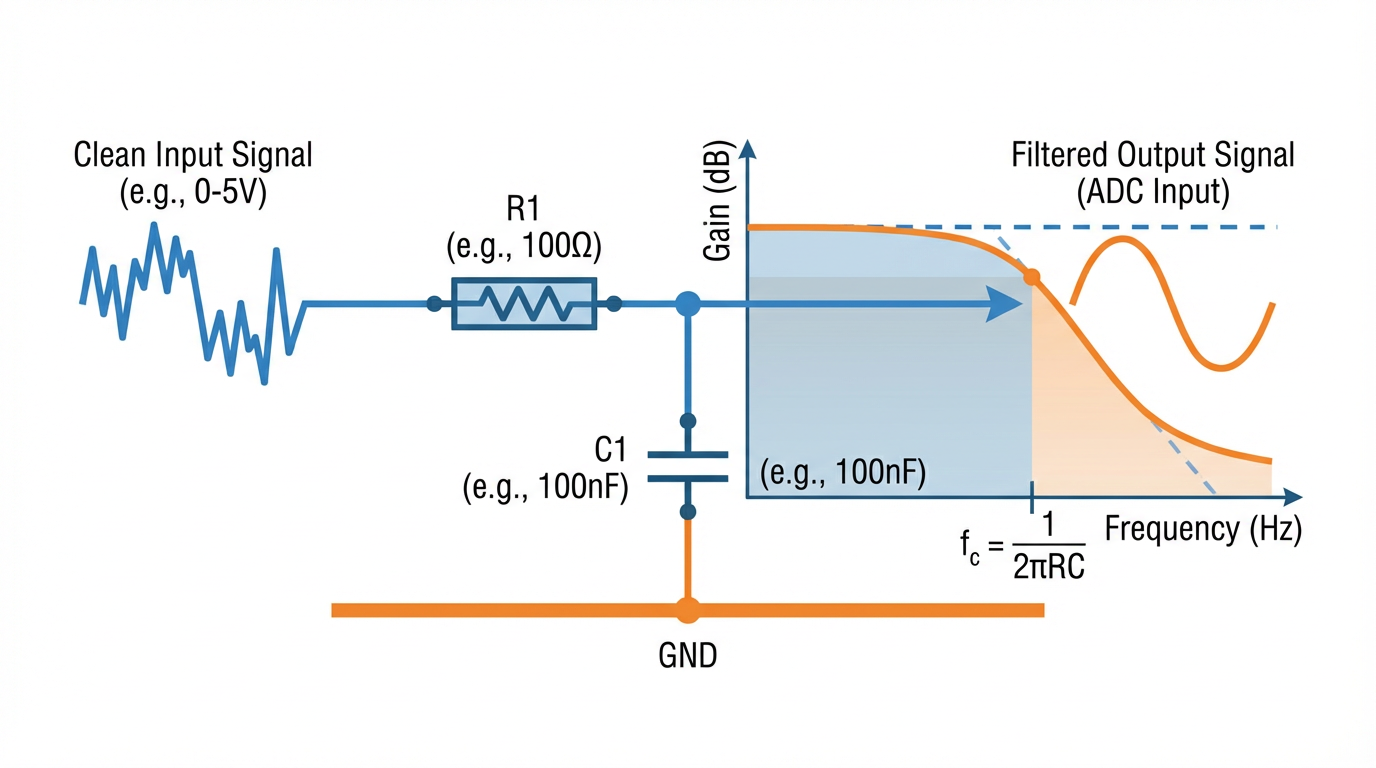
Input Filtering And ADC Acquisition
Noise at the ADC input does not just raise the noise floor; it can create conversion errors if the sampling network is not allowed to settle.
NXP recommends adding an external RC network at each ADC input: a series resistor from the signal source into the ADC pin and a capacitor from that pin to ground. This operates as both a low‑pass filter and a charge reservoir for the converter’s internal sample‑and‑hold capacitor.
Sizing that network is not arbitrary. NXP models the ADC input as a sampling resistance and capacitance and notes that incorrect external resistor and capacitor values can cause distortion because the internal capacitor does not fully charge during the allowed acquisition time. Their guidance is to account for acquisition time (which in their SAR example is roughly half the ADC clock period), internal and external capacitances, and the required accuracy so that the sampling capacitor settles to the target within a small fraction of an LSB.
Renesas reaches similar conclusions: keep the series resistor modest, place the capacitor physically close to the pin, and respect the ADC’s input impedance and timing requirements.
Done correctly, these filters both smooth noise and make the converter less sensitive to source impedance, which is a prerequisite for achieving 16‑bit‑class accuracy in multiplexed modules.
Reference Strategy And Ratiometric Techniques
The voltage reference is a quiet but central player in any accuracy budget. Monolithic Power Systems points out that the digital result is effectively the input voltage divided by the reference span and multiplied by the number of codes. Any noise or drift in the reference therefore directly appears as measurement error.
Analog Devices designs like the AD4111 include an internal reference but also allow external references when even tighter drift and noise are needed. They decouple the reference pin locally and route it away from switching nodes, treating it as its own sensitive network.
There is another powerful technique when sensor physics allow: ratiometric measurement. An Electronics Stack Exchange discussion distills this nicely. If a sensor’s output scales with its supply voltage, and you tie the ADC reference to that same supply, both the sensor output and the reference shift together. The ADC measures their ratio, not the absolute voltage, so changes in supply voltage cancel out. This is common with pressure sensors and strain gauges powered from the same rail as the ADC reference.
In such cases, adding a separate precision reference is often unnecessary. Instead, powering sensor and ADC reference from a common excitation voltage, as the discussion recommends, delivers stable digital readings even when the supply drifts within a reasonable band.
In a module claiming 16‑bit accuracy, you should expect the documentation either to lean on a robust reference architecture or to explain where ratiometric behavior is being used to cancel supply variation.

Accuracy Specifications In Datasheets: What To Look For
When you open a datasheet or product brief for an analog input module or its core ADC, you will see a mix of parameters. The trick is to link them to the real‑world behavior you care about.
Monolithic Power Systems and Contec both break down critical definitions.
Valid conversion range tells you the minimum and maximum input voltage the ADC can convert correctly. Converters may support unipolar ranges, where zero code corresponds to ground, or bipolar ranges, where negative full scale maps to the lowest code and positive full scale to the highest. Inputs beyond that range saturate at the nearest endpoint code.
Resolution, as discussed earlier, is the number of codes, not a guarantee of accuracy.
Offset error describes how far the converter’s output is shifted from zero at zero input. Gain error describes error in slope at full scale. Integral non‑linearity captures how far the actual transfer curve bends away from a straight line. Differential non‑linearity, which Contec and Monolithic Power Systems both explain, measures how much each step size deviates from one LSB; large negative differential non‑linearity can cause missing codes.
Conversion accuracy in Contec’s examples is specified in LSBs. For a twelve‑bit converter over a ±10 V span, they point out that one LSB corresponds to just under five millivolts, and a ±2 LSB accuracy specification means the converter could be roughly ten millivolts off anywhere in that range. For sixteen bits, the per‑step voltage is smaller, so the same LSB error specification corresponds to a tighter absolute error.
The analog front‑end and reference errors add on top. Analog Devices addresses this by publishing total unadjusted error figures for devices like the AD4111, chosen so typical system‑level requirements can be met without extensive calibration. Modules built around such parts may inherit these specifications, or they may add their own calibration and adjustment to tighten them further.
The key point is this: a credible “16‑bit accuracy” claim should be traceable back to explicit offset, gain, linearity, and noise specifications, expressed in LSBs or percent of full scale, and ideally to a tested EMC performance envelope like the AD4111 evaluation board’s immunity and emission results.
Specifying A 16‑Bit High‑Resolution Module For A Project
From an integration perspective, choosing or designing a 16‑bit‑class analog input module is less about chasing glamorous numbers and more about aligning realistic performance with your process requirements.
In practice, I start with the process variable. Contec’s explanation of resolution using temperature is a good mental model. You should decide what smallest change in signal you need to detect, over what range, and translate that into an equivalent number of steps. If your process only needs the equivalent of about twelve bits, spending money and engineering effort on sixteen bits may not be justified. Conversely, if your process needs better than sixteen bits, you must be honest about the complexity that entails and consider oversampling, averaging, or higher‑resolution converters.
Next, I verify that the module’s input ranges, as in the AD4111 and Speedgoat examples, match my field signals without wasting resolution. If most sensors are 4–20 mA, a module that treats current inputs as first‑class citizens is preferable to one that forces signal conditioning in the field.
Isolation strategy comes next. AllAboutCircuits’ distinction between module‑to‑backplane isolation and full channel‑to‑channel isolation is critical. If your wiring runs are long, your grounds are messy, or you expect frequent re‑wiring, channel‑to‑channel isolation, like that in Apex’s boards or in high‑end PLC cards, avoids subtle cross‑talk and fault propagation that can ruin accuracy.
Then I dig into the accuracy numbers. Using the definitions from Monolithic Power Systems and Contec, I check offset, gain, and linearity specifications, and I pay attention to conditions: temperature range, common‑mode range, input source impedance, and sampling rate. Where available, I look for noise‑free resolution or ENOB figures rather than raw resolution. Apex’s admission that their 24‑bit designs are engineered for about 16 bits of noise‑free resolution is refreshingly candid; that is the type of transparency I like to see in a vendor.
Finally, I look for evidence that the module’s layout, grounding, and EMC design follow the practices recommended by NXP, Cadence, Renesas, and ByteSnap. Evaluation board reports, like the EMC tests documented for the AD4111 reference design, are valuable here. So are architectural details such as per‑channel filters, local decoupling, and shielding similar to the metal‑can analog section Apex uses in their weigh‑scale boards.
When all of those pieces line up, a “16‑bit accuracy” spec starts to look like a realistic description of the module’s behavior rather than a marketing label on an ADC inside.
Short FAQ
Is 16‑bit resolution always necessary for industrial analog inputs?
Not always. Contec’s resolution examples show that many applications are well served with eight, twelve, or sixteen bits depending on required step size. For many temperature, level, and pressure measurements, twelve bits of true performance are enough. Higher resolution becomes valuable when small changes have large economic impact or when you intend to filter and average to capture subtle trends.
Why do some 24‑bit modules only claim about 16 bits of “noise‑free” performance?
Because real‑world noise, reference limitations, and front‑end errors eat into the ideal bit depth. Apex is explicit that their 24‑bit converters are engineered to yield about sixteen bits of noise‑free resolution in industrial conditions. That is common: overspecifying raw resolution at the silicon level gives you room to filter and average down to the noise floor you need at the system level.
How much does PCB layout really matter for a 16‑bit module?
It matters a great deal. NXP, Cadence, Renesas, and ByteSnap all show that poor grounding, long loop areas, inadequate decoupling, and careless routing can easily degrade effective resolution and accuracy by several bits. In my experience, it is entirely possible to turn a 16‑bit converter into a ten‑bit system just by ignoring layout best practices.
Getting to true 16‑bit‑class accuracy from a high‑resolution analog input module is less about chasing a single number and more about aligning specifications, architecture, and disciplined analog design. When you read the small print, lean on the kind of guidance provided by vendors like Contec, Analog Devices, NXP, and others, and apply the same rigor in your own layouts and system integration, you end up with measurement you can trust and a control system that behaves the way your operators expect every shift.
References
- https://www.plctalk.net/forums/threads/analog-module-resolution.1396/
- https://forum.pjrc.com/index.php?threads/general-beginner-best-practices-for-design-wiring-and-coding-teensy-3-1-joystick.27143/
- https://web-material3.yokogawa.com/GS34M06H11-04E.us.us.pdf
- https://apexembeddedsystems.com/pages/high-resolution-analog-input?srsltid=AfmBOooS0m56-NUJXDa_kZBquod2kKEI3NjnjHpwsIbtNmmx1yzn2Hqe
- https://resources.pcb.cadence.com/home/2020-analog-layout-basics-for-pcb-design
- https://controlbyweb.com/x418/?srsltid=AfmBOoq_2aX8AAzFVtwQDLa78zxIDRCyxleafaMR7S23cPwmggjNVy4u
- https://www.edn.com/how-to-maximize-performance-in-analog-input-modules/
- https://www.speedgoat.com/products/io-connectivity-analog-io109
- https://www.allaboutcircuits.com/industry-articles/plc-dcs-analog-input-module-design-channel-channel-isolation-high-density/
- https://www.bytesnap.com/news-blog/analog-design-12-tips-for-electronic-product-development/
Keep your system in play!
Top Media Coverage
Categories


Related articles Browse All
-
 amikong NewsSchneider Electric HMIGTO5310: A Powerful Touchscreen Panel for Industrial Automation2025-08-11 16:24:25Overview of the Schneider Electric HMIGTO5310 The Schneider Electric HMIGTO5310 is a high-performance Magelis GTO touchscreen panel designed for industrial automation and infrastructure applications. With a 10.4" TFT LCD display and 640 x 480 VGA resolution, this HMI delivers crisp, clear visu...
 -
 BlogImplementing Vision Systems for Industrial Robots: Enhancing Precision and Automation2025-08-12 11:26:54Industrial robots gain powerful new abilities through vision systems. These systems give robots the sense of sight, so they can understand and react to what is around them. So, robots can perform complex tasks with greater accuracy and flexibility. Automation in manufacturing reaches a new level of ...
 -
 BlogOptimizing PM Schedules Data-Driven Approaches to Preventative Maintenance2025-08-21 18:08:33Moving away from fixed maintenance schedules is a significant operational shift. Companies now use data to guide their maintenance efforts. This change leads to greater efficiency and equipment reliability. The goal is to perform the right task at the right time, based on real information, not just ...


- Q&A
- Policies How to order Part status information Shipping Method Return Policy Warranty Policy Payment Terms
- Asset Recovery
- We Buy Your Equipment. Industry Cases Amikong News Technical Resources Why choose us
- ADDRESS
-
 32D UNITS,GUOMAO BUILDING,NO 388 HUBIN SOUTH ROAD,SIMING DISTRICT,XIAMEN
Leave Your Comment