
-
Please try to be as accurate as possible with your search.
-
We can quote you on 1000s of specialist parts, even if they are not listed on our website.
-
We can't find any results for “”.
How to Select an Analog Input Module for Measurement Accuracy Needs

When a control system misbehaves, the problem is often not the PID tuning or the PLC logic. It is the analog input module quietly distorting the real world before your code ever sees it. After years of commissioning PLC and DCS systems in factories, labs, and test rigs, I have learned that getting the analog input choice right is one of the fastest ways to improve measurement accuracy and long‑term stability.
This article walks through how to choose an analog input module when accuracy really matters, using concepts and examples from vendors such as National Instruments, Analog Devices, Texas Instruments, Balluff, Contec, and others. The focus is practical: how to translate data sheet numbers into a module that actually meets your accuracy requirements in the field.
Accuracy, Resolution, and Noise: Getting Terms Straight
Before you can specify a module, you need to be precise about the word “accuracy.” Different vendors use different formulas, but the underlying ideas are similar.
National Instruments describes accuracy as how close the instrument reading is to the true value, while resolution is simply how finely the input range is divided into digital steps. NI and Contec both show that an N‑bit analog‑to‑digital converter (ADC) provides 2^N discrete codes. For a ±10 V span, a 12‑bit ADC has 4,096 codes, and each code is roughly a few millivolts wide; a 16‑bit ADC on the same range has 65,536 codes, with individual steps in the hundreds of microvolts. Resolution defines the smallest ideal code step, but it does not tell you whether the module can actually measure that finely once noise and other errors are included.
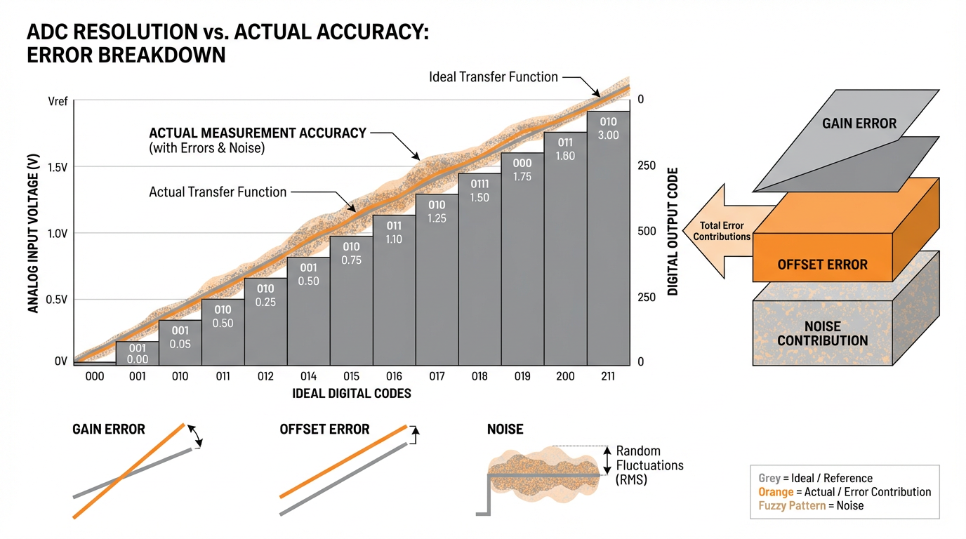
NI further distinguishes between resolution and absolute accuracy. For many data acquisition devices, absolute accuracy is expressed as a combination of a percentage of the reading, a percentage of the range, and sometimes a fixed number of counts. In a high‑precision DMM example, NI shows an accuracy of ±(20 parts per million of reading plus 6 parts per million of range), which translates to roughly a couple hundred microvolts of error when measuring around 7 V on a 10 V range. For DAQ devices, NI similarly aggregates gain error, offset error, nonlinearity, and noise into a single analog input accuracy number per range.
That same principle appears in NI’s guidance for dynamic signal acquisition devices. For a 1 kHz sine at 10 V on one such device, the manufacturer publishes separate maximum values for gain amplitude accuracy in decibels, offset, and flatness. NI converts each term into a voltage error and then sums them to get an overall analog input amplitude accuracy of about 38.75 mV. The important message is that accuracy is usually the sum of several error sources, not a single number like “16 bits.”
Balluff, in its discussion of “true analog” resolution for position measurement, underscores another key distinction: noise often dominates. In one example, a linear position sensor has a stroke of about 2.36 inches with a 0–10 V output and about 10 mV of system noise on the signal lines. Because 10 mV is one‑thousandth of the full‑scale voltage, the smallest practical position step you can resolve is around one‑thousandth of the stroke, roughly 0.0024 inches. Even if a 12‑bit ADC gives an ideal step size smaller than that, the real resolution is still set by the noise, not the nominal bit count.
Taken together, the vendor data show that you should treat “accuracy,” “resolution,” and “noise” as distinct. Resolution tells you what is theoretically possible; accuracy and noise determine what you will actually get.
Start With the Signal, Not the Module
Every good analog input selection starts at the field terminals. You need to be clear about what is coming in before you worry about the module’s part number.
Signal type and range
PPI India’s overview of analog input modules emphasizes signal compatibility as the first selection criterion. In process control work, the usual signals are voltage in ranges like 0–10 V or ±10 V, and current loops in ranges such as 4–20 mA. There are also specialized signals such as resistance inputs, strain‑bridge millivolt outputs, and temperature from RTDs and thermocouples.
Contec and NI both point out that a module’s input range should be matched to the sensor’s output range whenever possible. For example, Contec explains that a 0–5 V sensor measured on a 0–10 V range wastes half the available codes and doubles the effective step size. If you can configure the module for a 0–5 V range or amplify the signal to fill a 0–10 V range, you gain an immediate improvement in effective resolution.
PPI India extends this by recommending adjustable input ranges on each channel where possible, so that a single module can accommodate a mix of 0–10 V, ±10 V, and 4–20 mA loops without sacrificing measurement granularity.
Wiring, isolation, and grounding
Contec’s analog I/O fundamentals highlight another early decision: whether to use isolated inputs. Isolated analog input devices use photocouplers between the host and the I/O side, and sometimes isolation amplifiers per channel, to block ground potential differences and high‑frequency noise. This not only protects the controller but also improves measurement accuracy in noisy environments and multi‑ground systems.
In my own projects, isolated analog input modules have paid for themselves on long production lines where different machines sit on different ground references.
Non‑isolated modules in those cases often pick up enough common‑mode noise and ground loop current to show visibly jittery trends on pressure and temperature traces, even when the sensors are perfectly fine.
Contec also explains the difference between single‑ended and differential inputs. Single‑ended inputs share a common reference and use two wires per channel, which allows more channels but makes the system more sensitive to ground noise. Differential inputs use two signal wires plus ground per point; they offer superior noise rejection and are usually a better choice for long cable runs and low‑level signals, though they cut channel count roughly in half for a given module size.
When you select a module, verify from the data sheet whether the channels are single‑ended, differential, or software‑configurable, and whether bus isolation and channel‑to‑channel isolation are provided. Those structural choices directly affect how robust your measurements will be to plant noise.
Source impedance and input impedance
Even with the right range and wiring, the interplay between the sensor’s output impedance and the module’s input impedance can quietly ruin accuracy.
Microchip’s best‑practice guidance for ADC performance stresses that the source impedance must be low enough relative to the ADC’s sampling behavior that the internal sample‑and‑hold capacitor can charge properly. If the source impedance is too high, the converter will produce incorrect codes even if the nominal full‑scale range is correct. That is why high‑resolution ADC front ends often include buffer amplifiers rather than connecting sensors directly to the ADC pins.
On the module side, the input impedance is just as important. A discussion on the Arduino industrial Opta module shows a data‑sheet input impedance of about 8.9 kΩ and a measured impedance near 9 kΩ, which is unusually low for analog measurement. Participants there note that 100 kΩ or higher is more common on industrial analog modules. If you connect a high‑impedance transducer to an input that low, the module will draw noticeable current and create a voltage divider, adding a systematic error that no amount of digital filtering will fix.
Texas Instruments engineers, in a forum discussion on the ADS1220 ADC, approach the problem from the ADC perspective. They describe how the effective input impedance is derived from specified input currents and how, even when the programmable gain amplifier is bypassed, the input currents and thus the impedance remain relatively high for the preferred channels. The practical advice is to use the input pins with the lowest input currents when only a single channel is needed, because they yield the highest effective input impedance.
The lesson for module selection is straightforward. Check input impedance in the module data sheet and compare it with the sensor’s output impedance. For very high‑impedance sources, favor modules with high input impedance or integrated buffering; for medium‑impedance sources, make sure the ratio is high enough that the module’s loading error stays within your error budget.
Range, Resolution, and ADC Architecture Inside the Module
Once you understand the signals, you can turn to the module internals: ranges, ADC resolution, and converter architecture.
Matching range to the job
Contec’s examples highlight just how much range selection matters. For a 0–100 degree temperature span, they show that 8 bits (256 steps) give about 1 degree increments, 12 bits (4,096 steps) give about 0.1 degree increments, and 16 bits (65,536 steps) provide about 0.01 degree increments. The underlying concept applies just as well to flow, pressure, or position.
National Instruments’ DAQ selection guidance makes a similar point with voltage ranges. On a ±10 V range, a 12‑bit converter yields a least significant bit (LSB) of roughly 5 mV; a 16‑bit converter on the same range yields steps of a few hundred microvolts. There is no point paying for 24‑bit converters if your process only needs 1 degree or a few millivolts of temperature resolution, but there is also no reason to accept a device that cannot resolve the smallest change you care about.
PPI India therefore recommends combining an understanding of the process variable’s range and required precision with the module’s available ranges and resolution. Ideally, your sensor’s full‑scale span should map over most of the module’s range so that every bit is used productively.
Choosing bit depth with noise in mind
NI’s measurement fundamentals and Contec’s examples both reinforce that resolution sets a lower bound on detectable change, but noise and accuracy define the real limit. Balluff’s “true analog” discussion provides a concrete illustration: the position sensor with a 2.36 inch stroke, a 0–10 V output, and 10 mV of noise can only distinguish about one‑thousandth of the stroke, or roughly 0.0024 inches. Even if the controller’s analog input uses a 12‑bit ADC that ideally resolves about 0.00058 inches per code in that setup, the practical resolution remains about four times worse, because any change smaller than the noise amplitude is buried.
EleTimes’ exploration of PLC analog input module performance reinforces this idea from the converter side. They discuss how low‑noise operational amplifiers and instrumentation amplifiers help preserve the ADC’s effective resolution and increase the “noise‑free” number of bits you actually get. In their example calculations for an eighteen‑bit ADC, they use the nominal LSB voltage and simulate settling errors that are kept well below half an LSB, ensuring that dynamic behavior does not degrade the effective resolution.
NI likewise analyzes DAQ accuracy by combining gain error, offset, and noise uncertainty. The message across these sources is consistent: when you pick a module, look at both the nominal resolution and the specified accuracy and noise performance. A clean 16‑bit module with a tight absolute accuracy specification can easily outperform a noisy 24‑bit module with a loose error band.
SAR versus sigma‑delta converters in modules
Analog Devices compares three dominant ADC architectures—successive approximation (SAR), sigma‑delta, and pipelined—across application segments. For the kinds of analog input modules used in PLCs and process control, the real contenders are SAR and sigma‑delta.
Modern SAR converters, according to Analog Devices, are the workhorses for multiplexed data acquisition. Devices in this family offer around 8 to 18 bits of resolution with sampling rates up to the low megasamples per second, and they have no pipeline latency. A sample‑and‑hold captures the input, and a binary‑search algorithm resolves the code bit by bit. Because there is effectively no digital filter delay, SAR ADCs are extremely well suited to single‑shot, burst, and fast multiplexed measurements across many channels.
Sigma‑delta converters, by contrast, are optimized for high resolution at lower effective data rates. Analog Devices notes that modern sigma‑delta ADCs deliver around 16 to 24 bits of resolution with usable sample rates up to a few hundred hertz. They use oversampling, noise shaping, and digital filtering to push quantization noise out of the band of interest. Many industrial sigma‑delta devices also integrate programmable‑gain amplifiers that directly accept low‑level bridge and thermocouple outputs.
The trade‑off is that these digital filters introduce pipeline delay. After a step change or a channel switch, you must wait several output cycles before the measurement fully reflects the new input. That makes sigma‑delta converters less attractive for true single‑shot measurements and very low‑latency control.
For PLC analog input modules, EleTimes highlights SAR ADCs as an efficient choice when you want good resolution, low power, and fast, multiplexed sampling. On the other hand, Analog Devices’ AD4111—a 24‑bit sigma‑delta converter with an integrated analog front end for ±10 V and 0–20 mA signals—is clearly aimed at high‑accuracy process input cards where update rates in the tens of hertz are acceptable and precision is paramount.
The practical selection rule is to favor SAR‑based modules for fast, multiplexed, low‑latency control tasks, and sigma‑delta‑based modules for slower, high‑accuracy measurements where power‑line rejection and noise performance matter more than speed.
The Analog Front End: Op Amps, Filters, References, and Layout
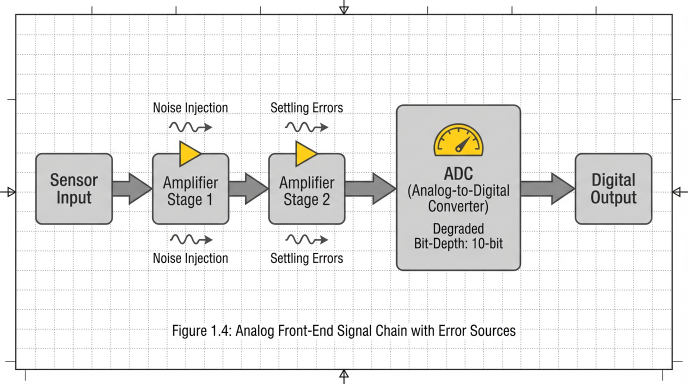
The ADC inside the module does not operate in isolation. The performance of the analog front end—the amplifiers, filters, references, supplies, and PCB layout—directly shapes the real‑world accuracy.
Input amplifiers and multiplexing behavior
EleTimes examines how the choice of amplifier affects PLC analog input performance, particularly in multiplexed systems where one ADC services several channels. When the multiplexer switches from one channel to another, large differential voltages can momentarily appear at the amplifier inputs, potentially forward‑biasing internal protection diodes. This creates leakage currents that slow the amplifier’s settling and degrade conversion accuracy, especially for high‑resolution converters.
The recommendation from that analysis is to use “multiplexer‑friendly” operational amplifiers that employ alternative protection schemes rather than simple input diodes. These devices handle fast channel switching without the slow leakage‑related settling behavior, so they can drive high‑resolution ADCs across many channels while still meeting LSB‑level accuracy.
EleTimes also distinguishes between MOSFET‑input or JFET‑input amplifiers and bipolar amplifiers. FET‑input devices offer very high input impedance and are therefore well suited for interfacing with high‑impedance field transmitters. JFET‑input amplifiers, however, may have narrower common‑mode input voltage ranges. Bipolar amplifiers generally deliver an excellent speed‑to‑power ratio with low noise, but they come with higher input bias currents and lower input impedance. Super‑beta transistor topologies in bipolar designs are highlighted as a way to improve both DC precision and AC performance, making them versatile choices for demanding PLC analog input architectures.
The conclusion is that you must consider both the sensor impedance and the multiplexing pattern when selecting or evaluating an input module. The wrong amplifier topology in the front end can quietly destroy the effective number of bits you thought you were buying.
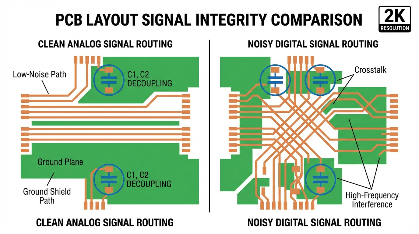
References, supplies, and layout discipline
Microchip’s best practices for improving ADC performance on microcontrollers transfer directly to analog input modules. They stress that the quality of the analog reference and the analog supply is critical. When the analog supply is shared with a digital supply, they recommend using an LC filter network between them, as described in the device data sheets. They also advise adding a capacitor between the reference pin and ground to improve stability, while respecting any limits on the voltage difference between analog and digital supplies.
On the PCB side, Microchip recommends keeping analog signal paths short and low‑impedance, routing them over a solid analog ground plane and away from high‑switching digital lines. They suggest adding decoupling capacitors between single‑ended signal inputs and ground, or between differential input pairs, with values chosen according to the signal bandwidth. During conversions, they recommend avoiding unnecessary toggling of I/O lines, especially those powered from the analog supply, and disabling digital input buffers on ADC pins to reduce injected noise. Where microcontroller features permit it, they suggest using noise‑reduction modes and oversampling to improve effective resolution and then applying offset and gain calibration to correct systematic errors.
Analog Devices’ application note on testing high‑speed ADCs reinforces the importance of clean signal sources, filters, clocks, and power supplies. They describe using low‑phase‑noise crystal oscillators as encode sources and carefully specified band‑pass and low‑pass filters to ensure that the measurement of ADC performance is not limited by the test setup. They also recommend low‑noise linear regulators for sensitive converter rails and carefully matched filter networks to control harmonic distortion.
Even though PLC analog input modules tend to run at much lower sample rates than RF data converters, the same principles apply. A module with a good ADC but poor reference decoupling, noisy clocking, or sloppy layout will never achieve its advertised accuracy.
Integrated front ends versus discrete designs
Analog Devices’ AD4111 is a good illustration of how much can be gained by integration. This 24‑bit sigma‑delta ADC integrates an analog front end that directly accepts ±10 V voltage inputs and 0–20 mA current inputs from a single 5 V or 3.3 V supply. The voltage inputs are accurately specified up to ±10 V, but the device can tolerate overrange voltages up to ±20 V while still converting, and it has absolute maximum ratings of ±50 V on the voltage pins. That kind of robustness is very attractive in industrial environments where mis‑wiring and fault conditions are common.
For each voltage input, the AD4111 includes a precision high‑impedance resistor divider of at least 1 MΩ. This removes the need for external ±15 V buffer amplifiers and discrete precision resistor networks, reducing both board space and the cost‑versus‑accuracy tradeoffs associated with discrete resistor matching. On the current side, the input range extends from slightly below zero to 24 mA, which covers standard 4–20 mA loops with margin near both ends.
The device also integrates a voltage reference and an internal clock, and it includes open‑wire detection that operates from the low‑voltage supply, eliminating the traditional requirement for higher pull‑up rails. Analog Devices specifies total unadjusted error (TUE) targets at the system level so that many modules built around this chip will not need additional calibration. When calibration is required, the close matching between channels allows a single‑channel calibration to benefit multiple inputs. Beyond accuracy, Analog Devices provides an EMC‑characterized reference PCB design, tested against IEC surge, electrostatic discharge, and radiated emission standards, which reduces design and compliance risk.
For a systems integrator, the takeaway is that modules based on highly integrated front‑end devices like this often provide more predictable accuracy and robustness than ad‑hoc designs using many discrete parts. When comparing analog input modules, pay close attention to whether the vendor bases the design on such components and whether they state a clear TUE number rather than just the raw ADC resolution.
Reading and Comparing Accuracy Specifications
With all of these pieces in mind, you can now read analog input module data sheets with a sharper eye. Several vendor documents provide a common vocabulary for key specs.
Contec, NI, and others use resolution (in bits) to describe how finely the module can divide its configured range. NI and Contec both show simple examples: eight bits give 256 steps, enough to represent a 0–100 degree span in one‑degree increments, while sixteen bits give over sixty‑five thousand steps, enough to show hundredth‑degree changes on the same span.
Accuracy or absolute accuracy is described by NI and Contec as the deviation from an ideal transfer function over a range. For an analog input, that often shows up as a combination of gain error, offset error, and nonlinearity, each expressed in LSBs or as percentages. Contec illustrates this for a 12‑bit, ±10 V device where one LSB is roughly 4.88 mV, so an accuracy of ±2 LSB corresponds to nearly 10 mV of possible error. NI shows similar calculations for both static DAQ devices and dynamic signal acquisition systems, including the earlier 38.75 mV example where gain, offset, and flatness errors are combined.
Noise‑free resolution and effective number of bits (ENOB) are brought out by EleTimes and the ADC testing guides from Monolithic Power Systems. They stress that ENOB and noise‑free resolution are often lower than the ideal bit count and that designers should evaluate them across temperature and supply variations. MPS describes how offset and gain errors can be characterized and then corrected through calibration, and how histogram and sine‑wave‑fitting tests are used to measure differential and integral nonlinearity. These tests are usually carried out in the ADC vendor labs, but they shape the data‑sheet numbers you see on modules.
Input range, input impedance, and isolation are covered by Contec and the Arduino industrial discussion. Input range must match the process signal; input impedance must be high enough that module loading does not add unacceptable error; isolation must be adequate for the expected common‑mode voltages and noise.
The table below summarizes how these terms are used by the vendors cited and why they matter when you choose a module.
| Spec term | How vendors describe it | Why it matters for analog input modules |
|---|---|---|
| Resolution (bits) | Number of digital codes; NI and Contec explain that N bits give 2^N levels | Sets the smallest ideal step size; must be fine enough for required measurement units |
| Accuracy / absolute accuracy | NI and Contec define as deviation from ideal transfer function over a range, combining gain, offset, nonlinearity, and noise | Determines how close readings are to true values across range and conditions |
| Noise‑free resolution / ENOB | EleTimes and ADC testing notes relate to effective usable bits after noise | Indicates how many bits of the nominal resolution remain after noise is considered |
| Input range | PPI India and Contec specify supported spans such as ±10 V, 0–10 V, 4–20 mA | Must match or be configurable to the sensor output for best resolution and accuracy |
| Input impedance | Arduino Opta discussion notes typical values near 9 kΩ for one device, 100 kΩ or more for others | High impedance minimizes loading error, especially with high‑impedance transducers |
| Isolation | Contec describes bus and channel isolation via photocouplers and isolation amplifiers | Reduces ground loops, improves noise immunity, and protects the controller |
When you compare modules, do not stop at the resolution line. Work through the absolute accuracy tables, understand how gain and offset errors are specified, and confirm that the worst‑case absolute error, including noise, is acceptable for your process.
Verifying and Maintaining Accuracy in the Field
Once a module is installed, you still need to verify that it meets its specifications under real conditions.
An Electrical Engineering Stack Exchange discussion on testing PLC current input modules lays out the classical approach. The usual method is to use a calibrator from a reputable manufacturer and have that calibrator itself regularly calibrated against a traceable reference by a specialized lab. In some cases, a combination of a stable voltage source and a precision resistor or a precision ammeter can substitute, but then the system accuracy is limited by the accuracy of those instruments and components.
The same discussion emphasizes that you must first know the official specifications you intend to test against, including ambient temperature, warm‑up time, and supply voltage conditions. You then compare those conditions to what your plant can realistically provide and to what your existing instruments can support. Any method that assumes or backs out the exact value of internal load resistors in the module is considered suspect; it is better to rely on external standards.
ADC testing guides, such as those provided by Monolithic Power Systems and Analog Devices, show that characterization in the lab uses carefully controlled signal sources, filters, clocks, and capture equipment. While you will not reproduce that level of rigor on a plant floor, the principles still hold. Use the cleanest possible source and reference instrument available, respect warm‑up and stabilization times, and if you perform offset and gain calibration in the controller, document and control the conditions under which it is done.
A Practical Selection Workflow
When I am specifying analog input modules for a new system, I follow a consistent sequence that echoes the vendor guidance discussed here.
First, I work with the process engineer to define the smallest meaningful change in each variable and the maximum measurement error we can tolerate. NI suggests five core questions for choosing DAQ hardware, including what signals you need to measure, how fast they change, how small a change you care about, and how much measurement error the application can accept. Those questions translate directly into required resolution, bandwidth, and accuracy for the analog input module.
Next, I list the signal types, ranges, and wiring constraints. This includes whether the signals are 0–10 V, ±10 V, 4–20 mA, thermocouples, RTDs, strain bridges, or others; whether they share grounds; and whether isolation is needed. Using guidance from PPI India and Contec, I map those to modules that support the correct ranges, input types, differential versus single‑ended modes, and isolation level.
Then I scrutinize the module data sheets. I look at resolution in bits, but I spend just as much time on absolute accuracy tables, noise‑free resolution, input impedance, and isolation ratings. I compare those numbers to the process requirements, using examples from NI and Contec to translate LSB‑level errors into measurement‑unit errors. I also check whether the module design appears to rely on integrated front‑end devices, like Analog Devices’ AD4111, that offer robust overrange protection, high input impedance, and well‑documented total unadjusted error.
After that, I consider the dynamics. If the application requires fast multiplexed sampling across many channels with low latency—for example, when combining multiple fast pressure or position signals for motion control—I favor SAR‑based modules as described by Analog Devices and EleTimes. If the application involves slow‑moving temperatures or pressures where accuracy and noise rejection matter more than speed, I lean toward sigma‑delta‑based modules with strong line‑frequency filtering and higher noise‑free resolution.
Finally, before signing off, I plan how the module will be verified and calibrated on site. I align that plan with the vendor’s recommended test conditions and, where possible, arrange access to a calibrator or precision meter. I also make sure the project includes provisions for reasonably clean power and sensible cable routing, reflecting Microchip’s layout and decoupling recommendations and the signal‑chain guidance from Analog Devices.
Brief FAQ
Is higher resolution always better for analog input accuracy?
Not necessarily. Contec’s and NI’s examples show that higher bit counts reduce the ideal LSB size, but Balluff’s position‑sensor case study demonstrates that output noise can easily dominate the practical resolution. EleTimes also emphasizes that low‑noise front‑end design is needed to achieve the effective number of bits promised by a high‑resolution ADC. If the combined noise and absolute accuracy of a module are worse than your required resolution, adding more bits does not help.
Do I really need isolated analog input modules?
In many industrial environments, yes. Contec’s description of isolated analog I/O devices explains how bus isolation and channel‑to‑channel isolation protect the controller and reduce the impact of ground potential differences and noise. In my experience, whenever signals travel any real distance, cross between power distribution zones, or come from instruments tied to different grounds, isolated inputs dramatically improve stability and reduce nuisance issues.
How should I interpret a single “accuracy” number on a module data sheet?
Treat it as the tip of an iceberg. NI’s DAQ and dynamic signal acquisition documentation shows that this number usually aggregates gain error, offset error, nonlinearity, and noise, and may vary with range and configuration. Look for detailed accuracy tables or total unadjusted error specifications, and compare those to the smallest change in your process that you care about. If the worst‑case error at your chosen range is larger than that smallest change, the module will not meet your accuracy needs without external calibration and signal conditioning.
In the end, choosing the right analog input module is less about chasing the highest bit count and more about understanding the full signal chain. If you respect the interaction between sensors, wiring, front ends, converters, and calibration, and you let the numbers from vendors like NI, Analog Devices, Microchip, TI, and others guide you, you will end up with measurements you can trust—and control loops that behave the way they should.
References
- https://pubs.aip.org/aip/rsi/article/88/9/094702/958420/Existing-methods-for-improving-the-accuracy-of
- https://ppiindia.net/choosing-the-right-analog-input-module/
- https://www.plctalk.net/forums/threads/math-to-determine-accuracy-of-analog-ai.75546/
- https://www.eletimes.ai/enhancing-analog-input-module-performance-in-plcs
- https://at.farnell.com/how-to-improve-analog-to-digital-converter-accuracy?srsltid=AfmBOoorBTD2nmNTj7AEMEXi-f9w_UUec4SM5e0DV_qX5hpXtWE5aybI
- https://forum.arduino.cc/t/opta-analog-input-accuracy/1136047
- https://www.balluff.com/en-us/blog/understanding-true-analog-resolution
- https://www.digikey.com/en/articles/use-careful-component-selection-topology-and-layout-for-signal-chain-accuracy
- https://onlinedocs.microchip.com/oxy/GUID-F670183D-C025-46C7-B7F5-9BAD389BF43F-en-US-3/GUID-C476E897-0FD2-4F5B-9B1E-674BB6F7E8B8.html
- https://electronics.stackexchange.com/questions/522169/testing-the-accuracy-of-a-plc-current-input-module-economical-approach
Keep your system in play!
Top Media Coverage
Categories


Related Products
-
 PROXPAC XL Proximity Transducer,MetricManufacturer: Bently Nevada
 -
 PM860 Processor Unit KitManufacturer: ABB
 -
I/O Network ModuleManufacturer: Reliance Electric
-
Dual Thrust Position MonitorManufacturer: Bently Nevada
-
3300 XL Standard Extension CableManufacturer: Bently Nevada
-
3300 XL 8 mm Proximity ProbesManufacturer: Bently Nevada
-
3300 XL 8 mm Proximity ProbesManufacturer: Bently Nevada
-
PROXPAC XL Proximity Transducer,MetricManufacturer: Bently Nevada
-
Digital Input ModuleManufacturer: ICS Triplex
-
3300 XL 8 mm Proximity ProbesManufacturer: Bently Nevada

Related articles Browse All
-
 amikong NewsSchneider Electric HMIGTO5310: A Powerful Touchscreen Panel for Industrial Automation2025-08-11 16:24:25Overview of the Schneider Electric HMIGTO5310 The Schneider Electric HMIGTO5310 is a high-performance Magelis GTO touchscreen panel designed for industrial automation and infrastructure applications. With a 10.4" TFT LCD display and 640 x 480 VGA resolution, this HMI delivers crisp, clear visu...
 -
 BlogImplementing Vision Systems for Industrial Robots: Enhancing Precision and Automation2025-08-12 11:26:54Industrial robots gain powerful new abilities through vision systems. These systems give robots the sense of sight, so they can understand and react to what is around them. So, robots can perform complex tasks with greater accuracy and flexibility. Automation in manufacturing reaches a new level of ...
 -
 BlogOptimizing PM Schedules Data-Driven Approaches to Preventative Maintenance2025-08-21 18:08:33Moving away from fixed maintenance schedules is a significant operational shift. Companies now use data to guide their maintenance efforts. This change leads to greater efficiency and equipment reliability. The goal is to perform the right task at the right time, based on real information, not just ...


- Q&A
- Policies How to order Part status information Shipping Method Return Policy Warranty Policy Payment Terms
- Asset Recovery
- We Buy Your Equipment. Industry Cases Amikong News Technical Resources
- ADDRESS
-
 32D UNITS,GUOMAO BUILDING,NO 388 HUBIN SOUTH ROAD,SIMING DISTRICT,XIAMEN
Leave Your Comment